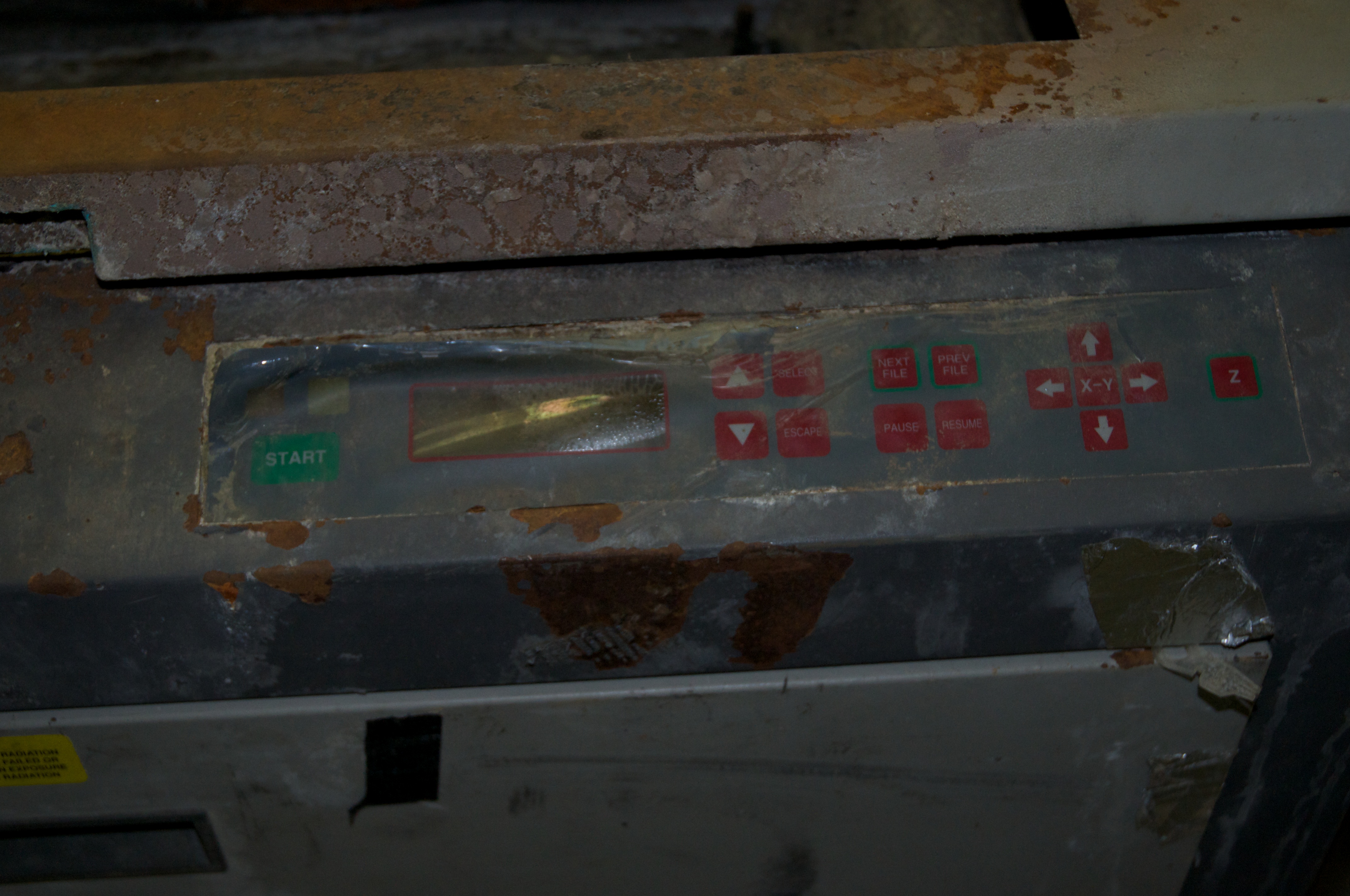
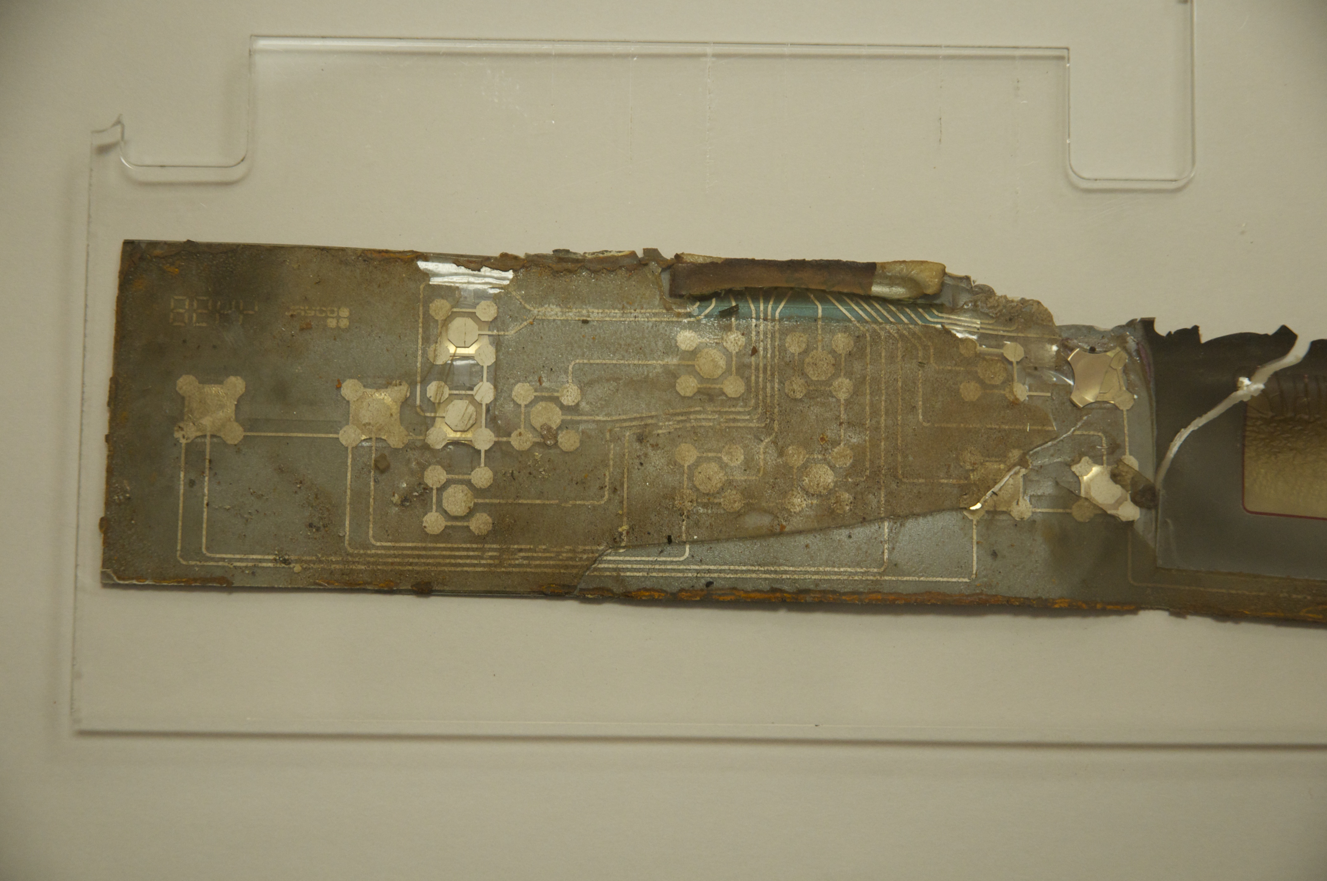
Today I took a bit of time after work to map out the membrane keypad of the control panel. Unfortunately it was badly burnt up, so unusable, and I didn’t take the best of care pulling it off.

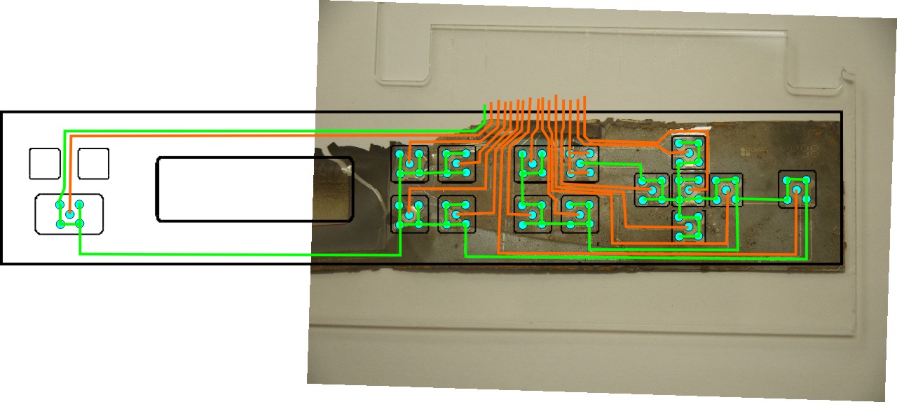
However, fortunately enough, it mostly came off in large pieces, so I was able to put the pieces together enough to trace out the signal mapping. to make life a little easier, I took a picture from the backside where the traces can be seen, and then traced out the lines in CorelDraw. Virtually any membrane keypad can be reverse engineered this way, as they are almost always printed on transparent material.

This image was then flipped and super-imposed & aligned onto a scale image of the control panel I pulled from a ULS manual, and then finally traced. I probably could have done it on paper, or just by eye, but this helped me keep track of where I was, and what was left to do.


Only two pins remained in question [1 & 2], and that is because that part of the membrane is completely gone. I knew what their signals were, but not what order they come out. Having said that, I chose the most logical ordering, leaving me with the following mapping.
1: Common
2: Start
3: Menu Up
4: Select
5: Menu Down
6: Escape
7: Z
8: Pause
9: Next File
10: Resume
11: Right Arrow
12: Down Arrow
13: Left Arrow
14: Prev File
15: Up Arrow
16: X-Y
Grabbing what was left of the controller board that the membrane attaches to, I was able to confirm that pin 1 is indeed the common, and is likely attached to ground. It is directly connected to the plane on the bottom of the board, I won’t know for sure if this is VCC or ground until I try to reverse engineer the board… but most commonly it would be connected to ground, with the individual switch lines pulled up to VCC via a resistor.
For those interested in membrane keypad construction, it is actually quite simple, and even possible to manufacture your own at home. [especially if you have a laser cutter ;)] The bottom layer of film has the circuit pattern printed on it using silver ink. The pattern includes all the traces, and pads for the buttons. More complex designs may use multiple layers, but most will do it on a single layer. If making one at home, you can print your pattern on paper and then using a conductive ink pen trace the pattern onto the plastic sheet [or plot it using a plotter & a conductive ink pen for a better result]. Laminated onto the bottom sheet is a second sheet of thicker plastic to act as a spacer [or use multiple layers of the thinner plastic]. This sheet has holes cut where the button domes go, as well as channels between the button locations. The channels are to allow for air movement when a button is pressed. Otherwise it’ll be like trying to squeeze a balloon flat when the user tries to press a button. Next metal domes are placed in each of the button locations. [home builders can get these domes from Digikey, of course your pattern has to be made to match the dome you are using] On top of this is another thin sheet of plastic with only holes cut for the tops of the domes, this holds everything together. Finally the graphic layer is applied. This is usually a back-printed film with all the necessary graphics on it. and that’s pretty much it. For the home builder I’d print on some photo paper, and then glue this onto the rest of the stack, it won’t be as durable, but should work. For some extra durability, you can have it laminated first.
In part 2 will be reverse engineering the front-panel controller/LCD board. This will be a challenge, as the PCB is virtually burnt black, and falling apart in places. It also has quite a few traces. Luckily it is also only a 2 layer PCB, and has minimal components, which I can identify, so that should help simplify things a bit.
Leave a comment